- 您现在的位置:买卖IC网 > Sheet目录117004 > 534CB000154BGR (SILICON LABORATORIES) CRYSTAL OSCILLATOR, CLOCK, 45.8752 MHz, CMOS OUTPUT
Si534
6
Rev. 1.0
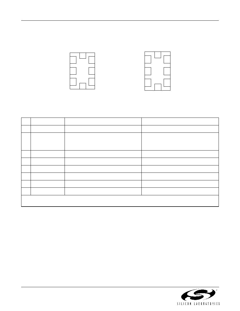
2. Pin Descriptions
Table 9. Pin Descriptions
Pin
Symbol
LVDS/LVPECL/CML Function
CMOS Function
1
NC
No connection
2OE*
Output enable
0 = clock output disabled (outputs tristated)
1 = clock output enabled
Output enable
0 = clock output disabled (outputs tristated)
1 = clock output enabled
3
GND
Electrical and Case Ground
4
CLK+
Oscillator Output
5
CLK–
Complementary output
No connection
6VDD
Power Supply Voltage
7
FS[1]*
Frequency Select MSB
8
FS[0]*
Frequency Select LSB
*Note: FS[1:0] and OE include a 17 k
value ordering.
(Top View)
LVDS/LVPECL/CML
CMOS
1
2
3
6
5
4
GND
OE
VDD
CLK+
CLK–
NC
FS[1]
FS[0]
7
8
1
2
3
6
5
4
GND
OE
VDD
CLK
NC
FS[1]
FS[0]
7
8
发布紧急采购,3分钟左右您将得到回复。
相关PDF资料
530HC982M000DGR
CRYSTAL OSCILLATOR, CLOCK, 982 MHz, CMOS/TTL OUTPUT
530JA119M000DG
CRYSTAL OSCILLATOR, CLOCK, 119 MHz, CMOS OUTPUT
530NA870M000DGR
CRYSTAL OSCILLATOR, CLOCK, 870 MHz, LVDS OUTPUT
530CB32M0000BGR
CRYSTAL OSCILLATOR, CLOCK, 32 MHz, CMOS OUTPUT
531FA388M000DG
CRYSTAL OSCILLATOR, CLOCK, 388 MHz, LVDS OUTPUT
531BB273M000DGR
CRYSTAL OSCILLATOR, CLOCK, 273 MHz, LVDS OUTPUT
531BB297M000DG
CRYSTAL OSCILLATOR, CLOCK, 297 MHz, LVDS OUTPUT
531FA944M000DG
CRYSTAL OSCILLATOR, CLOCK, 944 MHz, LVDS OUTPUT
相关代理商/技术参数
534CB000155DG
制造商:Silicon Laboratories Inc 功能描述:SMD CRYSTAL OSC 20.48MHZ/21.2992MHZ/22.1184MHZ/22.9376MHZ 3. - Trays
534CB000545DG
功能描述:标准时钟振荡器 QUAD XO 8 PIN 0.3PS RS JTR RoHS:否 制造商:AVX 产品:Standard Clock Oscillators 封装 / 箱体:7 mm x 5 mm 频率:75 MHz 频率稳定性:50 PPM 电源电压:2.5 V 负载电容: 端接类型:SMD/SMT 最小工作温度:0 C 最大工作温度:+ 70 C 输出格式:LVDS 尺寸: 封装:Reel 系列:
534CB000545DGR
制造商:Silicon Laboratories Inc 功能描述:OSCILLATOR - Tape and Reel
534CB000558DG
功能描述:标准时钟振荡器 QUAD XO 8 PIN 0.3PS RS JTR RoHS:否 制造商:AVX 产品:Standard Clock Oscillators 封装 / 箱体:7 mm x 5 mm 频率:75 MHz 频率稳定性:50 PPM 电源电压:2.5 V 负载电容: 端接类型:SMD/SMT 最小工作温度:0 C 最大工作温度:+ 70 C 输出格式:LVDS 尺寸: 封装:Reel 系列:
534CB000558DGR
制造商:Silicon Laboratories Inc 功能描述:OSCILLATOR - Tape and Reel
534CB000578DG
功能描述:标准时钟振荡器 QUAD XO 8 PIN 0.3PS RS JTR RoHS:否 制造商:AVX 产品:Standard Clock Oscillators 封装 / 箱体:7 mm x 5 mm 频率:75 MHz 频率稳定性:50 PPM 电源电压:2.5 V 负载电容: 端接类型:SMD/SMT 最小工作温度:0 C 最大工作温度:+ 70 C 输出格式:LVDS 尺寸: 封装:Reel 系列:
534CB622080BG
制造商:SILABS 制造商全称:SILABS 功能描述:CRYSTAL OSCILLATOR (XO) (10 MHZ TO 1.4 GHZ)
534CB622080BGR
制造商:SILABS 制造商全称:SILABS 功能描述:CRYSTAL OSCILLATOR (XO) (10 MHZ TO 1.4 GHZ)